Recent Research Accomplishments in the Evans Research Group (link)
Recent Research Nuggets
Archived Research Nuggets
Ultrafast Piezoelectricity and Switching in Ferroelectric Oxides
Sub-Nanosecond Mechanical Response
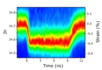
Ultra-fast time-resolved x-ray microdiffraction helped us recently
to reveal the local lattice dynamics of a PZT thin film device. The PZT
(002) Bragg peak position during a 10 ns long electrical pulse
presented on the plot demonstrates a sub-nanosecond response with a
mechanical strain of about 0.35%. This property can readily be used for
chopping singular x-ray bunches out of the sinchrotron x-ray beam for
further use in beam choppers. The time-resolved x-ray microdiffraction can be
applied to a broad range of problems of the ultra-fast lattice
dynamics.
D.-H. Do, P. G. Evans, E. D. Isaacs, D. M. Kim, C.-B. Beom Eom and E. M. Dufresne, Nature Materials 3, 365 (2004). (local) (publisher)
Supported by Department of Energy, Office of Basic Energy Sciences (link)
Structural and Electronic Properties of Silicon Nanomembranes
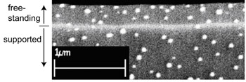
The heteroepitaxial growth of Ge on thin Si membranes can lead to significant bending under self-assembled Ge hut nanostructures. Undercut silicon-on-insulator mesas approximate a Si freestanding membrane and serve as a crystalline substrate for the growth of Ge huts. Synchrotron x-ray microdiffraction shows a local curvature on the lateral scale of the size of the hut and an overall bending of the freestanding region. In comparison with conventional mechanically rigid substrates, the freestanding film can bend significantly. We have found a local radius of curvature of 6 microns beneath huts on 30 nm-thick Si membranes.
P. G. Evans, D. S. Tinberg, M. M. Roberts, M. G. Lagally, Y. Xiao, B. Lai, and Z. Cai, Appl. Phys Lett. 87, 073112 (2005). (local) (publisher)
P. G. Evans, P. P. Rugheimer, M. G. Lagally, C. H. Lee, A. Lal, Y. Xiao, B. Lai and Z. Cai, J. Appl. Phys. 97, 103501 (2005). (local) (publisher)
Supported by the University of Wisconsin Materials Research Science and Engineering Center (link)
Single-Molecule-Thick Organic Semiconductor Electronics
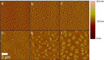
We have been working on organic field effect transistors (OFETs) based on pentacene and rubrene thin
films deposited on SiO2 substrates. Pentacene (C22H14) has high charge carrier mobility in thin films
and single crystals and forms robust, stable, transistor structures. We have studied the formation
of the pentacene channel and its relationship to the evolution of 2D growth of a pentacene monolayer
nd proved the drain current starts to flow at a sharp threshold where the pentacene islands come into
contact with each other during the initial stage of the transistor formation. Rubrene (C42H28) is one
f the prominent organic materials because of its relatively high values of the surface carrier mobility.
In comparison to pentacene, rubrene shows 3D growth of the circular islands even in the early stages
of growth. Morphology study is performed using atomic force microscopy in ambient air. It is essential
to link the electrical properties to the geometric effects of a semiconductor to understand the formation
of the conducting channel in an organic thin film transistor.
Supported by the University of Wisconsin Materials Research Science and Engineering Center and by the Petroleum Research Fund of the American Chemical Society. ( link)